
The Department of Commerce and Natcast, which operates the National Semiconductor Technology Center (NSTC), have announced the selection process for the first three research and development (R&D) facilities funded by the CHIPS and Science Act.
These facilities include an NSTC Prototyping and National Advanced Packaging Manufacturing Program (NAPMP) Advanced Packaging Piloting Facility, Administrative and Design Facility and Extreme Ultraviolet (EUV) Center. Information about the selection process for other affiliated technical centers will be announced later.
CHIPS for America investments aim to create a robust semiconductor industry in the U.S., supporting advanced R&D and creating well-paying jobs. Connecting research with industry ensures the lasting success of the initiative. The CHIPS R&D facilities will bring together partners from across the semiconductor ecosystem, enabling large-scale commercialization of technological advancements in semiconductor design and manufacturing.
“To reclaim America’s semiconductor leadership, we can’t just invest in manufacturing capacity; we also need to supercharge our research and development ecosystem,” Commerce Secretary Gina Raimondo said. “The National Semiconductor Technology Center and National Advanced Packaging Manufacturing Program are critical components in making that happen, and with the facilities CHIPS for America will be funding we will drive innovation and help recruit and train the next generation of American semiconductor workers.”
Once operational, these three cutting-edge facilities are positioned to become premier domestic destinations for advanced semiconductor R&D. They seek to address key current deficiencies in the industry, providing value to a range of stakeholders including universities, small businesses, large manufacturers and government agencies. Commerce and Natcast anticipate the NSTC Administrative and Design Facility being operational by 2025, the NSTC EUV Center by 2026 and the NSTC Prototyping and NAPMP Advanced Packaging Piloting Facility by 2028.
The facilities will enable collaboration to tackle the most complex challenges in microelectronics:
Accelerate innovation by providing R&D capabilities across all areas of microelectronics, including access to EUV lithography for research with advanced patterning technology.
Offer value to the semiconductor ecosystem beyond what existing facilities provide.
Ensure financial sustainability by attracting investments from companies of all sizes.
Maintain independence and neutrality, allowing Natcast, on behalf of the NSTC and the NAPMP, to make operational decisions and help member entities and their employees innovate.
Be part of ecosystems that support and grow a talented workforce and a robust network of semiconductor companies, educational and research institutions, and local support to advance their mission.
The CHIPS R&D facilities are driven by several principles, more than a year of stakeholder discussions, insights from the NSTC Vision and Strategy Paper, the NAPMP Vision Paper and a thorough analysis of current and future U.S. semiconductor manufacturing and R&D.
The NSTC Prototyping and NAPMP Advanced Packaging Piloting Facility will bring together cutting-edge manufacturing, packaging and next-generation technology development, offering NSTC members and NAPMP-funded researchers access to 300mm research, prototyping and packaging capabilities. Building out both in a single facility will allow for industrywide collaboration.
The Administrative and Design Facility will similarly bring together essential NSTC operations. It will accommodate Natcast’s administrative functions, provide a space for consortium members to work together and house additional programs.
The EUV Center will enable extensive research and a route to commercialization for NSTC members for next-generation technology development. The center will also provide space for Natcast researchers, staff and member assignees to conduct research and collaborate.
Commerce and Natcast will choose facilities that best align with the objectives of CHIPS for America based on an evaluation of relevant factors in each selection process.
An “Ecosystem Questionnaire for States and Territories to Inform CHIPS R&D Facility Site Selection Process” will be distributed next week to the Economic Development Organizations (EDOs) of all 56 states, territories and the District of Columbia. The questionnaire will look to identify semiconductor ecosystems that could support the NSTC Prototyping and NAPMP Advanced Packaging Piloting Facility. EDOs will be notified when the questionnaire is available and will have one week to complete it to be considered for the facility.
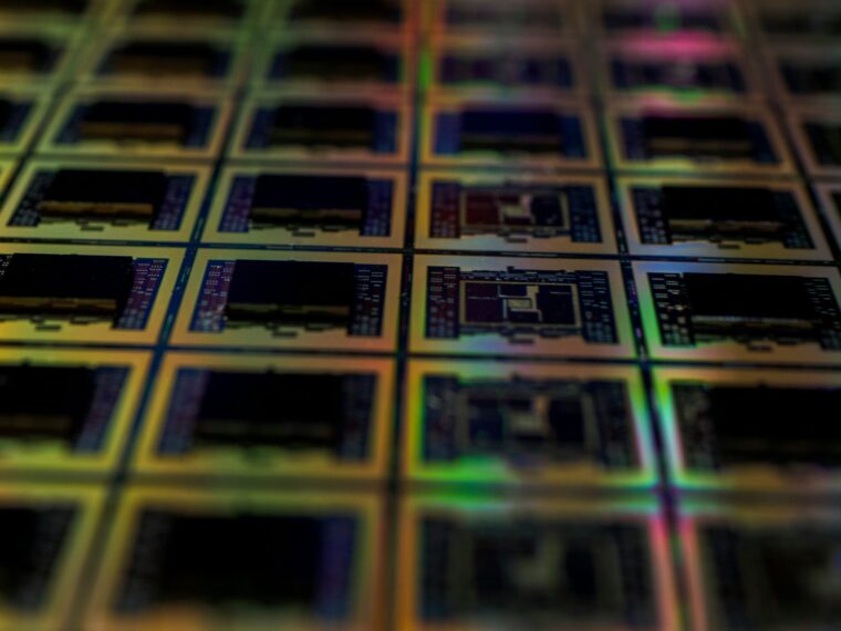
Photo by Maxence Pira on Unsplash
The post Commerce seeking partners for three facilities to advance semiconductor research appeared first on Government Market News.